
Spot Melting in Thin Wall Builds
Introduction
Here we report the results of the simulations of thin walls built with electon beam on a substrate.
Simulation Parameters
The Inconel 625 powder is used, the particle size is 45–105 micron.
The beam power is 270 W, the voltage is \(U=60\) kV, the current is \(I\)
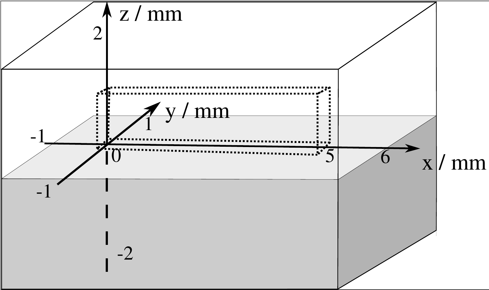
Fig. 78 Schematic of the simulation domain. The wall is represented by dotted lines.
The walls are built with 25 layers, and with one single track thickness at each layer. The length of the walls is 5 mm, the platform step is 50 micron.
We examine the three building strategies:
Continuous scan with the same scan direction on each layer (FF).
Continuous scan with the alternating back and forth scan direction (BF) on each layer.
Spot melting scanning (SM).
In the first and the second case, the beam speed is constand on each layer, \(S=0.6\) m/s.
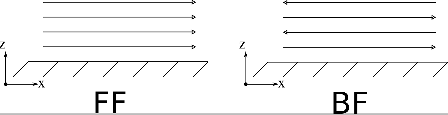
Fig. 79 Beam path in the FF and the BF case.
In the third case, the beam jumps on a series of discrete spots, making 5 passes on the wall at each layer. The distance between spots is \(d_s=100\) micron, the jump distance is \(d_j=500\) micron, and the total scan time of each layer is the same as in the FF an BF cases.
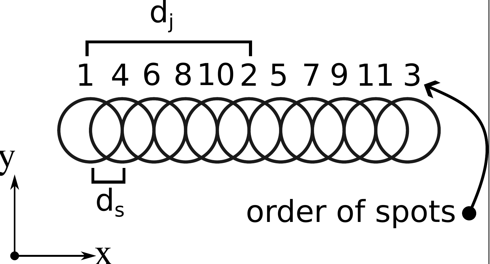
Fig. 80 Spots position and order schematic
Input
The input files are generated with scritps for multilayer procedure. Below is the input file for the first layer of the SM case.
{
  "outputDir": "./drop",
  "ScanStrategy": {
      "Beam": {
          "type": "Ebeam",
          "ElectronsEnergy": 60000.0
      },
      "Type": "XYpositions",
      "XYpositions": {
          "sourceFile": "../SpotMeltingScan.dat"
      }
  },
  "Camera": {
      "AmbientGas": "Ar",
      "pressure": 0.4,
      "temperature": 293.0
  },
  "NumericalParams": {
      "dr": 4e-06,
      "dt": 5e-08
  },
  "config": {
      "MemoryAllocation": "managed",
      "AllowToRunoutXYbox": true,
      "calcGrains": true,
      "StopIfGrainsLimitBoxReached": false,
      "DumpARR": false,
      "DumpVTK": false,
      "calcBubbles": false,
      "AutoTermination": true
  },
  "Substrate": {
      "preheating": 1000,
      "initGeometryVDBfile": "",
      "initialNucleiDensity": 1000000000000000.0
  },
  "Powder": {
      "initSpheresVDBfile": "init_spheres.vdb",
      "wettingAngle": 105
  },
  "PowderBedGenerator": {
      "Type": "PowDEM",
      "GroundSurface": "",
      "KnifeZposition": 0.0021,
      "PSDsizes": [ [ 0, 4e-05 ], [ 30, 5e-05 ], [ 45, 6e-05 ], [ 50, 7e-05 ], [ 55, 8e-05 ], [ 70, 9e-05 ], [ 100, 0.0001 ] ]
  },
  "licenseFile": "/licence.lic",
  "sizes": {
      "substrate": 0.002,
      "FullXapprox": 0.007,
      "FullYapprox": 0.002,
      "FullZapprox": 0.004,
      "GrainsLimitBox": [
          [ 0.0005, 0.0005, 0.0015 ],
          [ 0.0065, 0.0015, 0.0035 ]
      ]
  },
  "Visual": {
      "RenderOnlyMeltpool": false,
      "3DrenderedDomainSize": [ 0.002, 0.001, 0.001 ]
  },
  "Material": "Inc625_micro"
}
In the simulation, the grains growth is turned on in the material parameters of the Inc625_micro material.
The grains are initialized in the substrate (density is \(10^{15}\) per \(m^3\)) in the domain limited by the GrainsLimitBox parameter, and in the powder particles.
The scanning path is set via external file. See here for the manual on this feature.
This is the beginning of the SpotMeltingScan.dat file. You can download it here.
0 0.001 0.001 270 0.00025
0.0001633986928104575 0.001 0.001 270 0.00025
0.00016389869281045752 0.0015 0.001 270 0.00025
0.000327297385620915 0.0015 0.001 270 0.00025
0.00032779738562091503 0.002 0.001 270 0.00025
0.0004911960784313726 0.002 0.001 270 0.00025
0.0004916960784313725 0.0025 0.001 270 0.00025
0.00065509477124183 0.0025 0.001 270 0.00025
0.00065559477124183 0.003 0.001 270 0.00025
0.0008189934640522874 0.003 0.001 270 0.00025
...
The first column is time in seconds, the second and the third are the position of the beam at this time. The positions between the time instants which are specified in the file, are interpolated between the closest values. The remaining two columns are the power and the spot size at this time.
Results
Typical time of simulation of one layer is 5 hours. Full set of simulations (3 walls, 25 layers) lasted about a week using 3 GPUs.
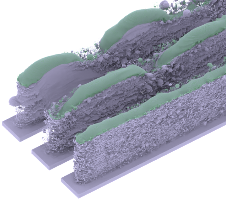
Fig. 81 Wall shapes for the FF, BF and SM cases in that order.
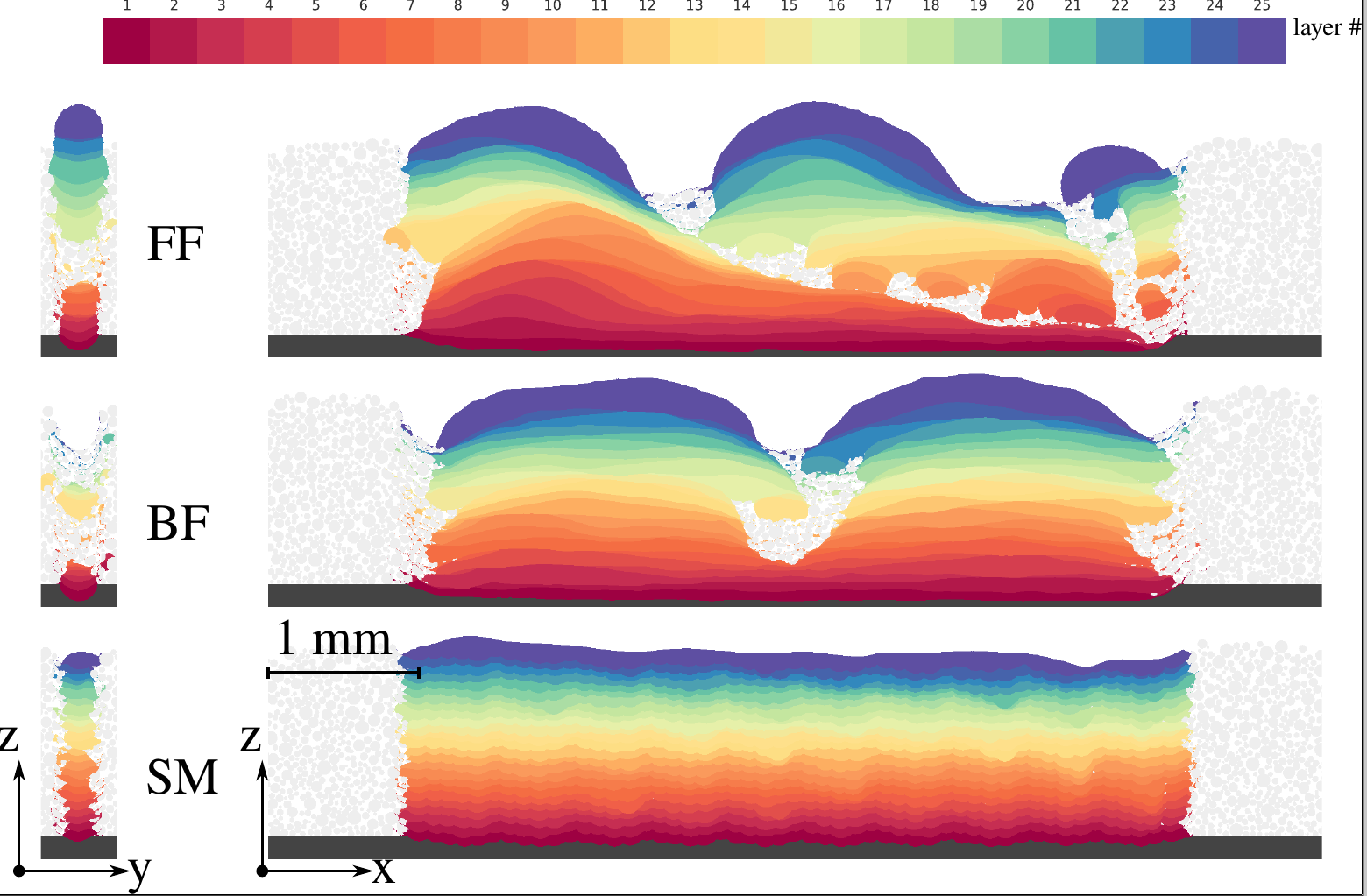
Fig. 82 Longitudinal cross-section of the walls.
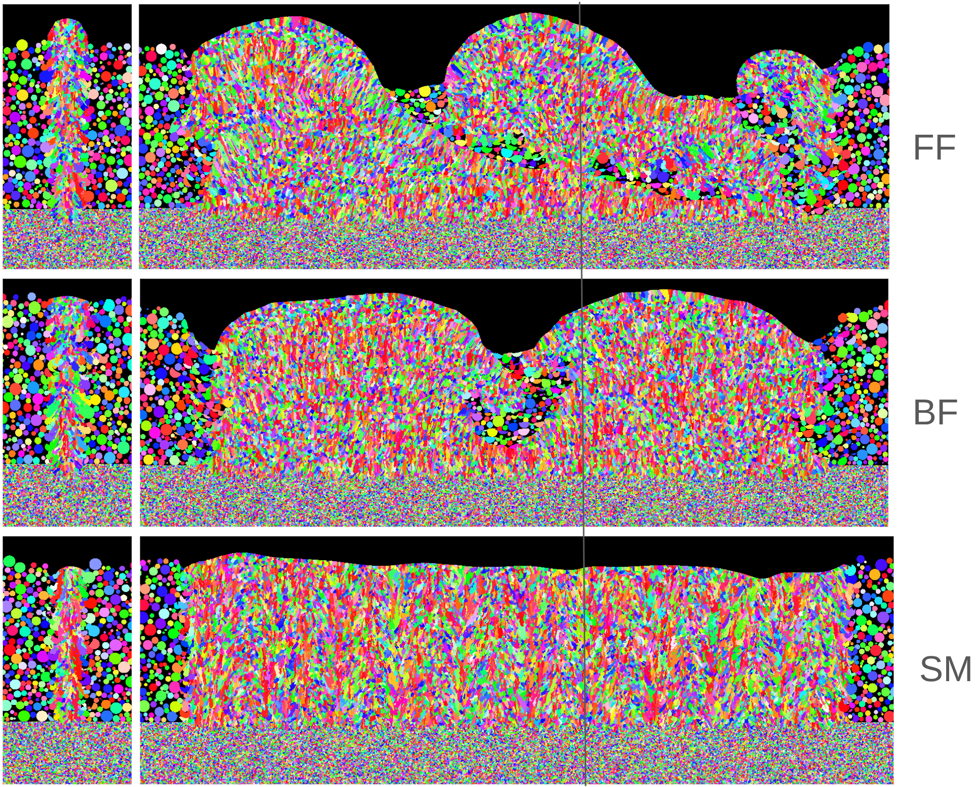
Fig. 83 Grains structure in the transverse and longitudinal cross-sections of the walls.
Fig. 84 Back and force continuos scanning. Click on the image to view the video
Fig. 85 Spot melting. Click on the image to view the video
We conclude that the thin wall morphology is strongly dependent on scan strategy, with the best morphology obtained with the spot melting. It is explained by more equally distributed energy input along the wall profile, resulting in more stable melt pool. Spot melting could be a way to improve the morphology of thin wall builds